
LCD/OLED Repair
Laser repair of process defects in LCD and OLED panel manufacturing
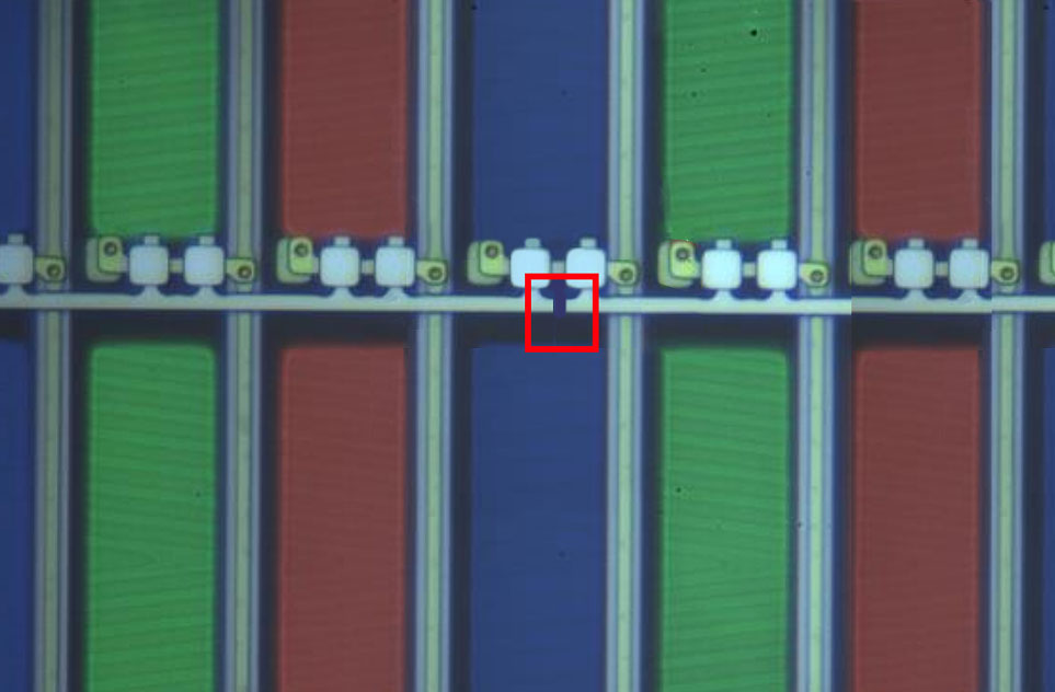
During the manufacturing of LCD and OLED panels, various defects such as bright spots, dark spots, flashing points, and fragmented bright spots may occur. These defects can lead to poor display quality in certain areas. However, they can be repaired or mitigated through laser processes such as circuit cutting, welding, and darkening. By repairing or mitigating these defects with laser technology, the yield of panel products can be improved, significantly reducing the production costs for panel manufacturers.
more
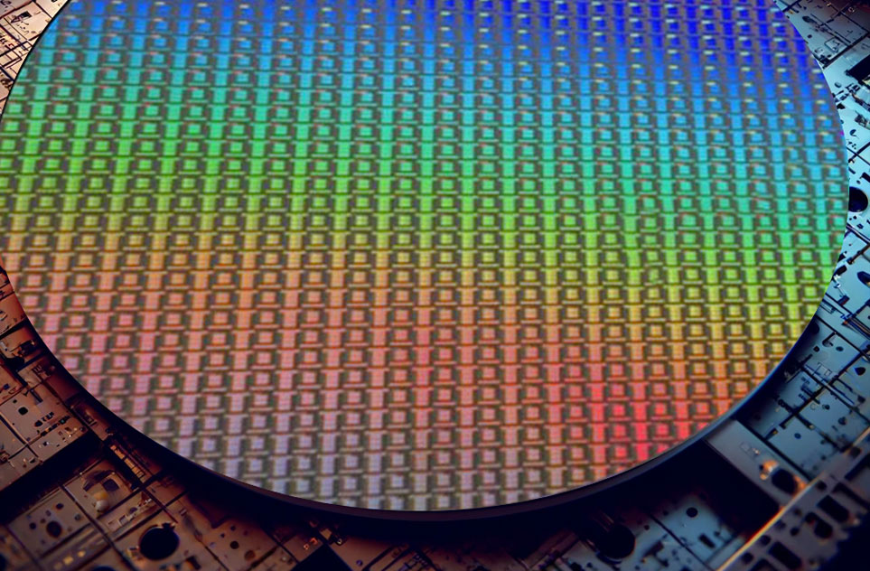
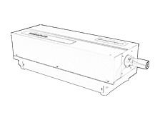
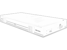
Wafer Annealing
One of the key auxiliary technologies in the field of semiconductor manufacturing
Laser wafer annealing is a critical technology used in semiconductor manufacturing. It employs a high-power laser source to heat the surface layer of the wafer to high temperatures in an extremely short time, followed by rapid cooling. This process can significantly improve lattice defects and grain boundary issues in the wafer, enhancing the crystalline quality and crystal orderliness. The laser annealing technology is favored in the semiconductor industry for its advantages, such as localized heating, precise temperature control, high energy density, and continuous stable output. These benefits allow it to meet various annealing process requirements, making it a powerful method to effectively enhance product performance and yield in semiconductor manufacturing.
more
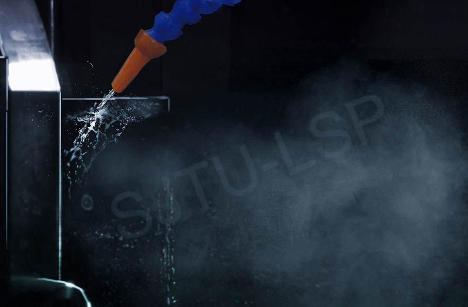
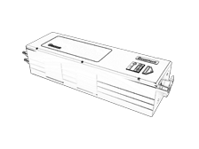
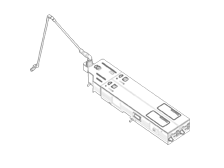
Laser Shock Peening
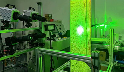
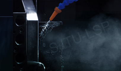
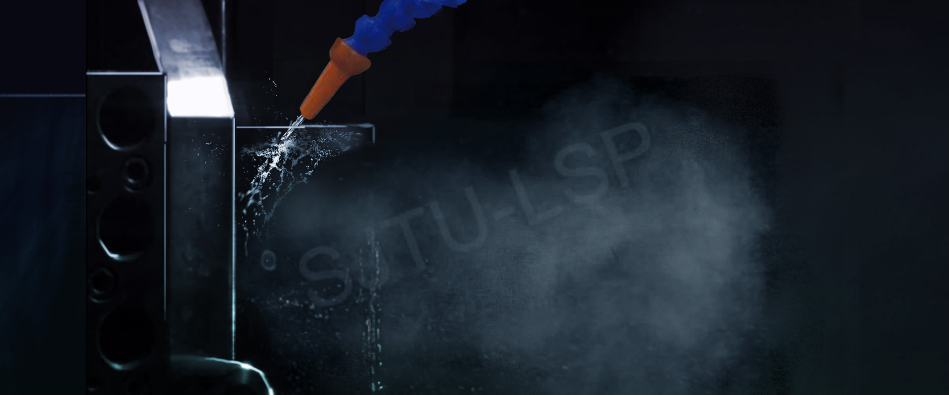
Laser technology enhances the fatigue resistance, wear resistance, and corrosion resistance of metal materials
is a high-tech method that uses high power density, short-pulse lasers (in the range of 10 to 30ns) to generate high-intensity shock waves on the material surface by applying an absorbing layer that absorbs the laser energy. This process induces high residual compressive stress, improves the initiation life of fatigue cracks, effectively reduces the driving force for fatigue crack propagation, and extends the fatigue crack propagation life.
more