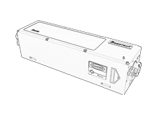
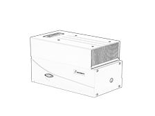
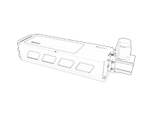
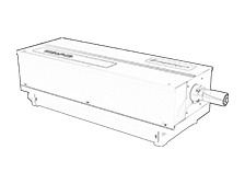
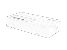
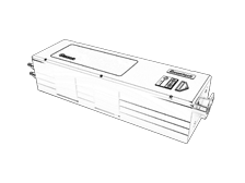
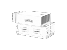
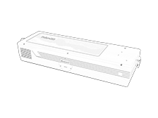
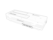
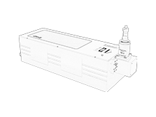
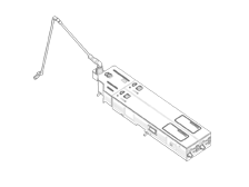
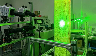
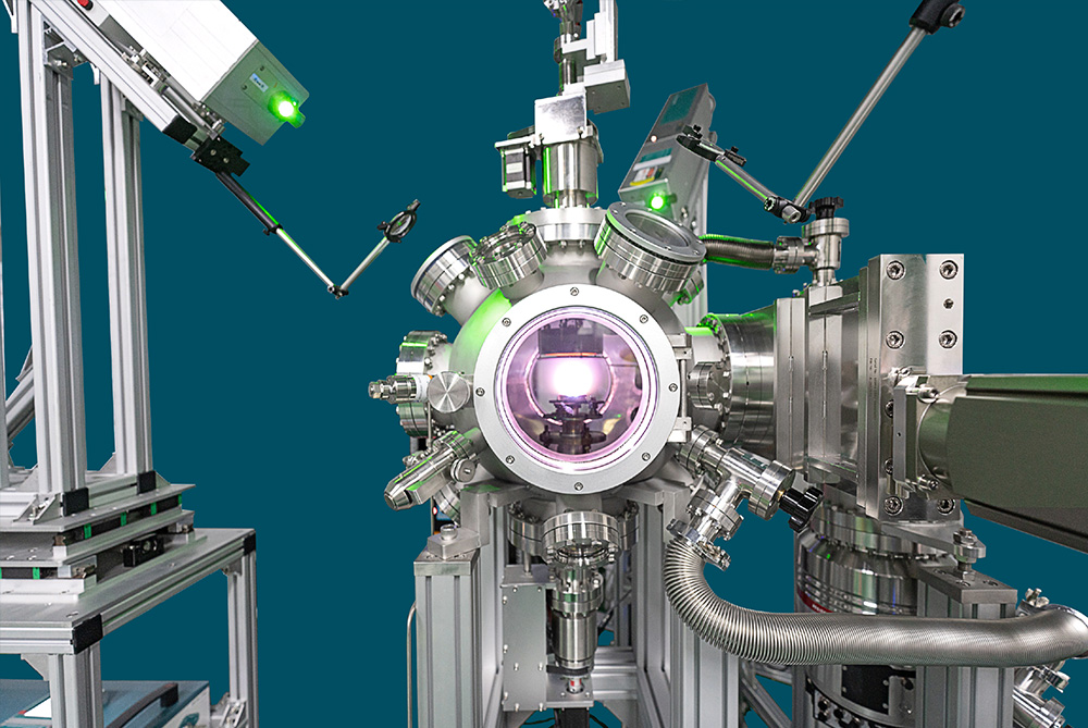
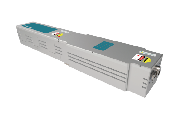
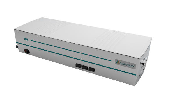
Pulsed Laser Deposition (PLD) is a technique that uses a laser to bombard a target material, causing the ejected material to deposit on various substrates and form coatings or thin films. A typical PLD system mainly consists of a vacuum chamber and pulsed laser. The laser is focused onto the target material in the vacuum chamber through appropriate lenses. The choice of laser wavelength depends on the target material, with commonly used wavelengths being 266 nm, 355 nm, and 248 nm. Some materials also require 532 nm and 1,064 nm lasers.
A client has developed a triple-beam pulsed laser co-deposition system using the intelligent Nimma-HG-Pro pulsed solid-state laser developed by Beamtech Optronics Co., Ltd. for the preparation of large-size superconducting thin films. Superconductors are known as the "highways" for unobstructed electron movement. How can superconducting materials be made thinner and finer than one-hundredth of a human hair? Under a high-energy laser beam, the high temperature of 3,000°C can instantly alter the material's state, ultimately depositing to form a palm-sized thin film. The superconducting chips made from this process are faster and consume less energy. In the future, 7G, 8G, and even more advanced communication technologies can be realized through this innovation.

