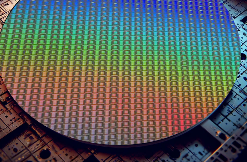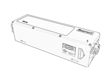
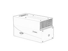
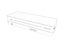
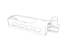
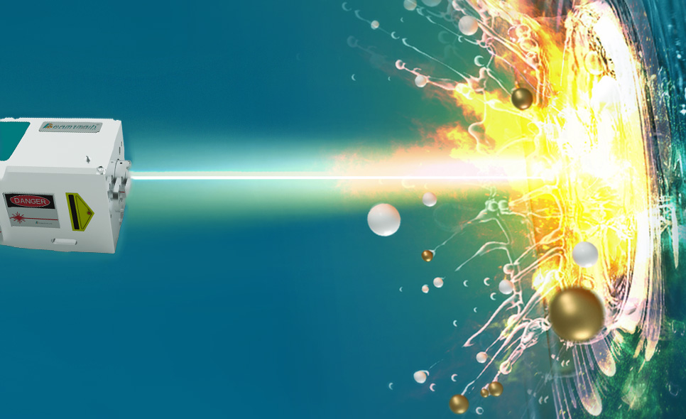
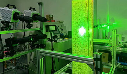

Laser wafer annealing is a critical technology used in semiconductor manufacturing. It employs a high-power laser source to heat the surface layer of the wafer to high temperatures in an extremely short time, followed by rapid cooling. This process can significantly improve lattice defects and grain boundary issues in the wafer, enhancing the crystalline quality and crystal orderliness. Laser annealing technology is favored in the semiconductor industry for its advantages such as localized heating, precise temperature control, high energy density, and continuous stable output. These benefits allow it to meet various annealing process requirements, making it a powerful method for effectively enhancing product performance and yield in semiconductor manufacturing.
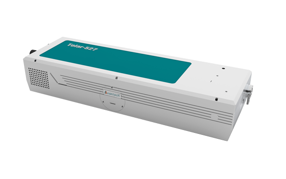
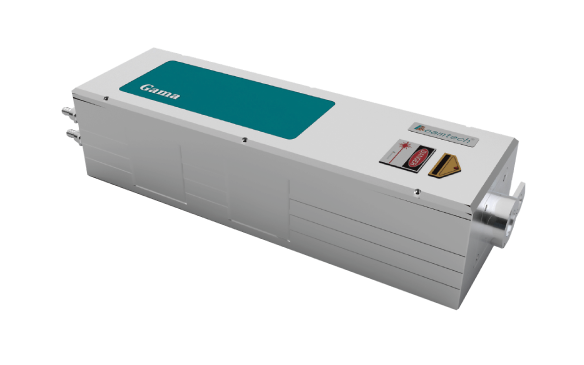
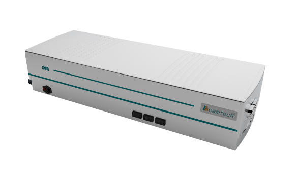
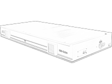
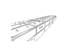
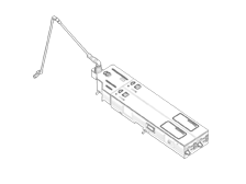
应用推荐产品